Fully integrated Photonic design automation

PIC Different.

One connected place to design, simulate, lay out, and verify photonic integrated circuits.

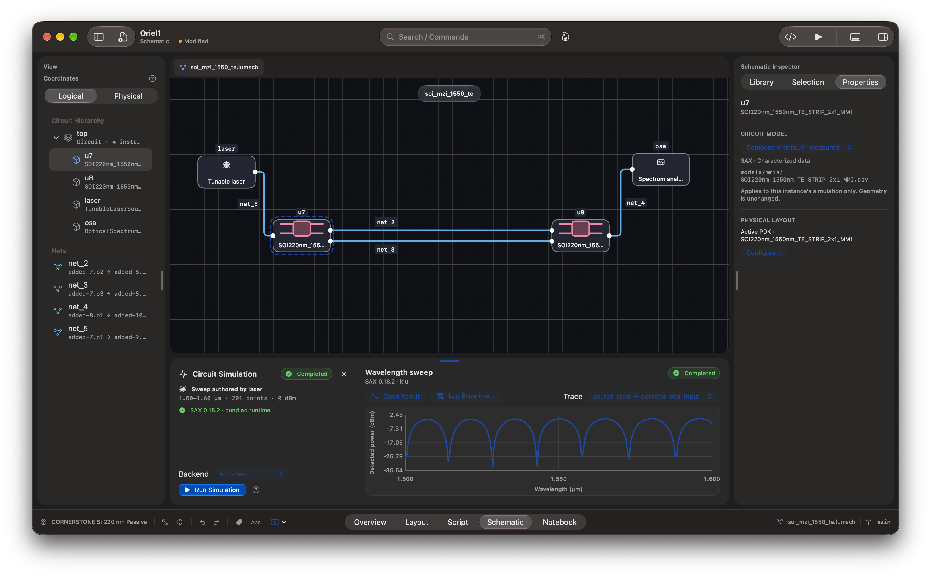
Lumicron for Mac showing an Oriel1 photonic circuit schematic and a saved wavelength sweep
DESIGN STUDIO / MAC Circuit, simulation, layout, and verification.
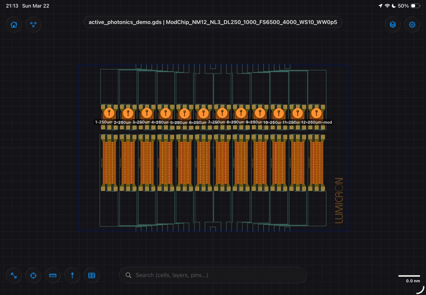
Lumicron iPad companion showing a photonic chip layout and device pins
LAB COMPANION / IPAD Navigate the chip at the probe station.

Built for Apple silicon. Designed for photonics.

From circuit
to physical design.

Work with the circuit as an engineering system—not a collection of disconnected files.

  1. 01

    Simulate

    Understand the circuit first

    See behavior before committing to layout.

    Run SAX simulations beside the schematic and save the result in the same project. Sweeps, traces, and design context remain connected.

    Oriel1 project notebook showing a saved wavelength sweep beside its circuit
    Oriel1 · saved wavelength sweep
    Circuit simulation
  2. 02

    Layout

    Write less layout plumbing.

    Express more design intent.

    Describe the layout the way you think about it. Place components relative to one another, connect named ports, and let the PDK carry the routing details. Lumicron’s layout API is designed to turn engineering intent into physical geometry without burying it in coordinate math.

    Complete PCellElyon Demo PDK
    @lm.pcell
    def MZI(
        span: float = 300,
        imbalance: float = 60,
    ):
        c = lm.CELL("MZI")
        splitter = c.add(
            pdk.NxM_MMI(n_inputs=1, n_outputs=2))
        combiner = c.add(
            pdk.NxM_MMI(n_inputs=2, n_outputs=1))
    
        (c.Place(combiner).right_of(splitter)
           .move_by(span, 0))
        c.Route(
            splitter.ports["o2"],
            combiner.ports["i2"],
            profile=pdk.RP.silc_strip)
        (c.Route(
            splitter.ports["o1"],
            combiner.ports["i1"],
            profile=pdk.RP.silc_strip)
           .jog("S", by=imbalance))
        return c
    Readable circuit intentGenerated physical layout
    Lumicron layout viewerNamed ports · PDK route profile
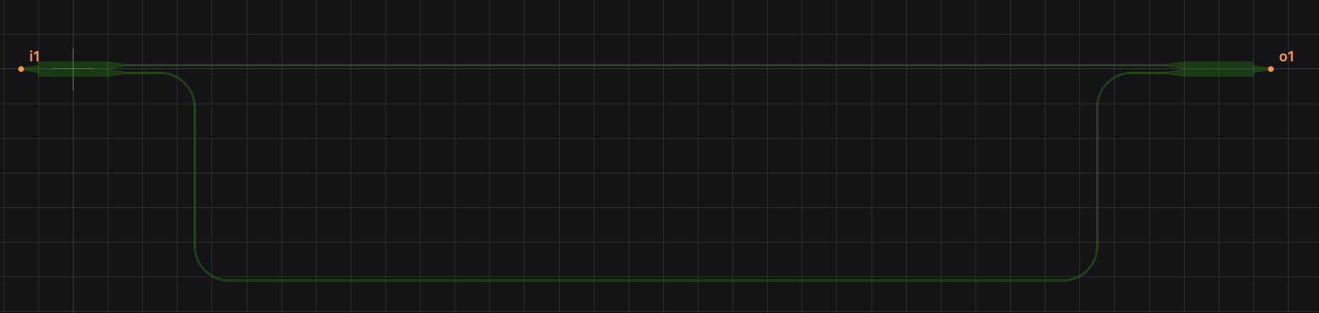
    The MZI generated by the Lumicron PCell shown above, open in Lumicron’s layout viewer with named input and output ports
    The complete PCell above generated this MZI in Lumicron. The PDK supplies the optical routing geometry and process layers.
    Python · PDKs · GDS/OASIS
  3. 03

    Verify

    Close the loop.

    Check the layout against fabrication rules and circuit intent.

    DRC

    Check supported process rules using the project or PDK verification deck.

    LVS

    Compare the physical implementation against the intended circuit connectivity.

    DRC · Authored LVS

Why Lumicron exists

Photonic design should
feel like one discipline.

The design record should travel with the work—from schematic and simulation to physical layout, verification, and the lab.

  1. 01Schematic + Simulation
  2. 02Layout + Verification
  3. 03Lab

Engineering continuity
is the point.

The work moves between views. The project retains what the engineer meant.

01

One project.
One thread of intent.

Open your project and see what exists, what ran, and what still needs verification. Design files, the active PDK, saved simulations, and Phoebe stay together so the next decision starts with the whole project in view.
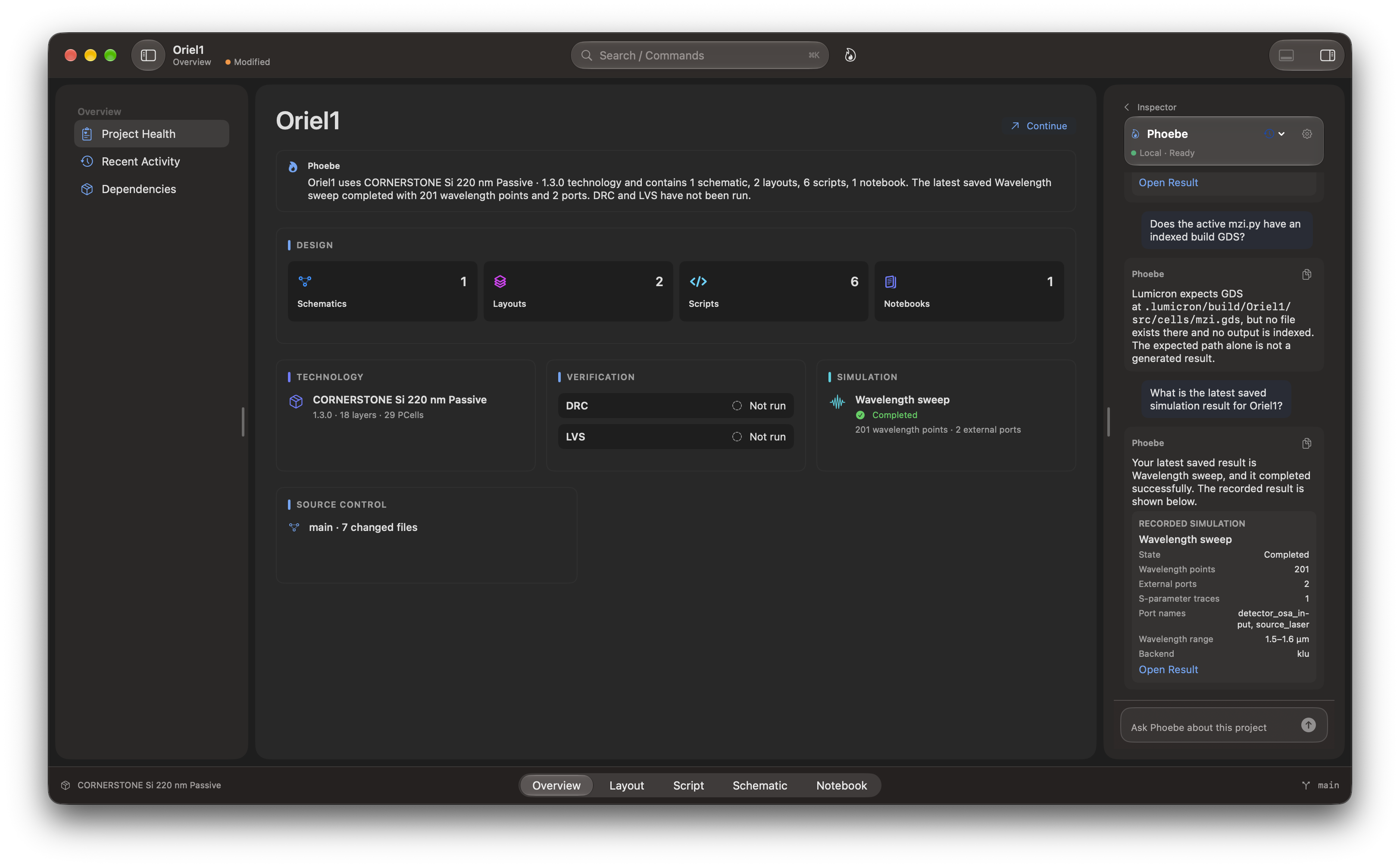
Oriel1 project overview showing its files, saved simulation, PDK, verification state, and Phoebe together
Oriel1 · project overview
02

Layout remembers
what it is.

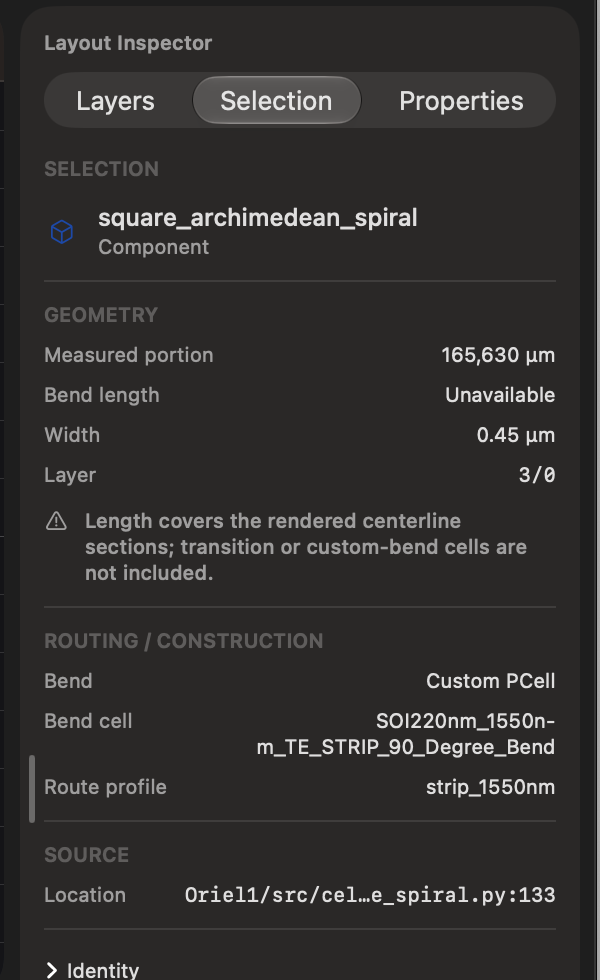
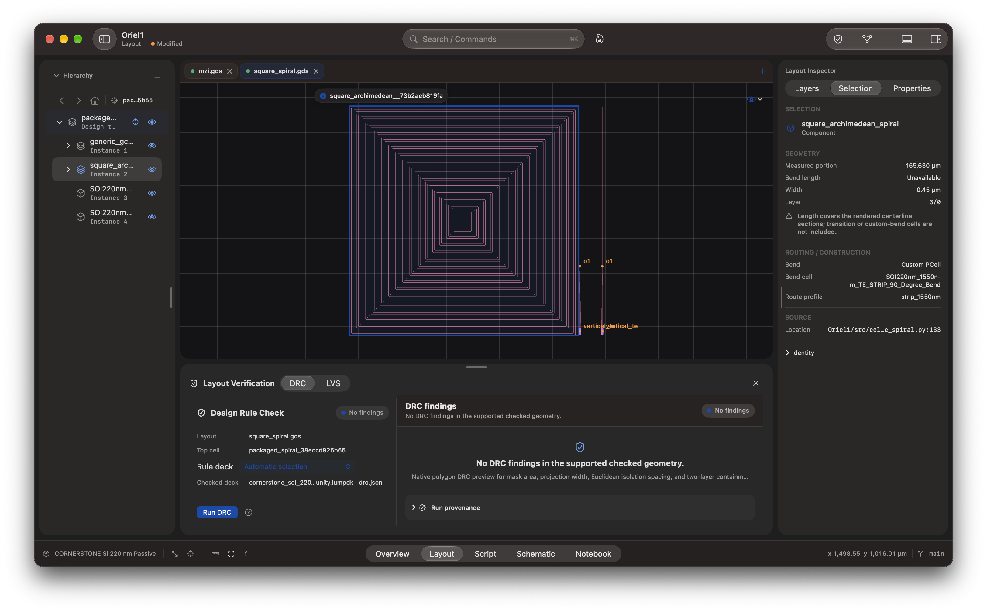
Lumicron Oriel1 layout with a selected spiral and Layout Inspector visible
Layout Inspector165,630 µm measured
Layout Inspector selection and geometry: square_archimedean_spiral, measured portion 165,630 micrometers, width 0.45 micrometers, layer 3/0
Route profile strip_1550nm and Oriel1 source location in the real Layout Inspector
Select a physical component and inspect the engineering data behind it. Lumicron keeps dimensions, component identity, PDK routing context, and source provenance attached to the layout.

Mac native

Direct when you want it.
Programmable when you need it.

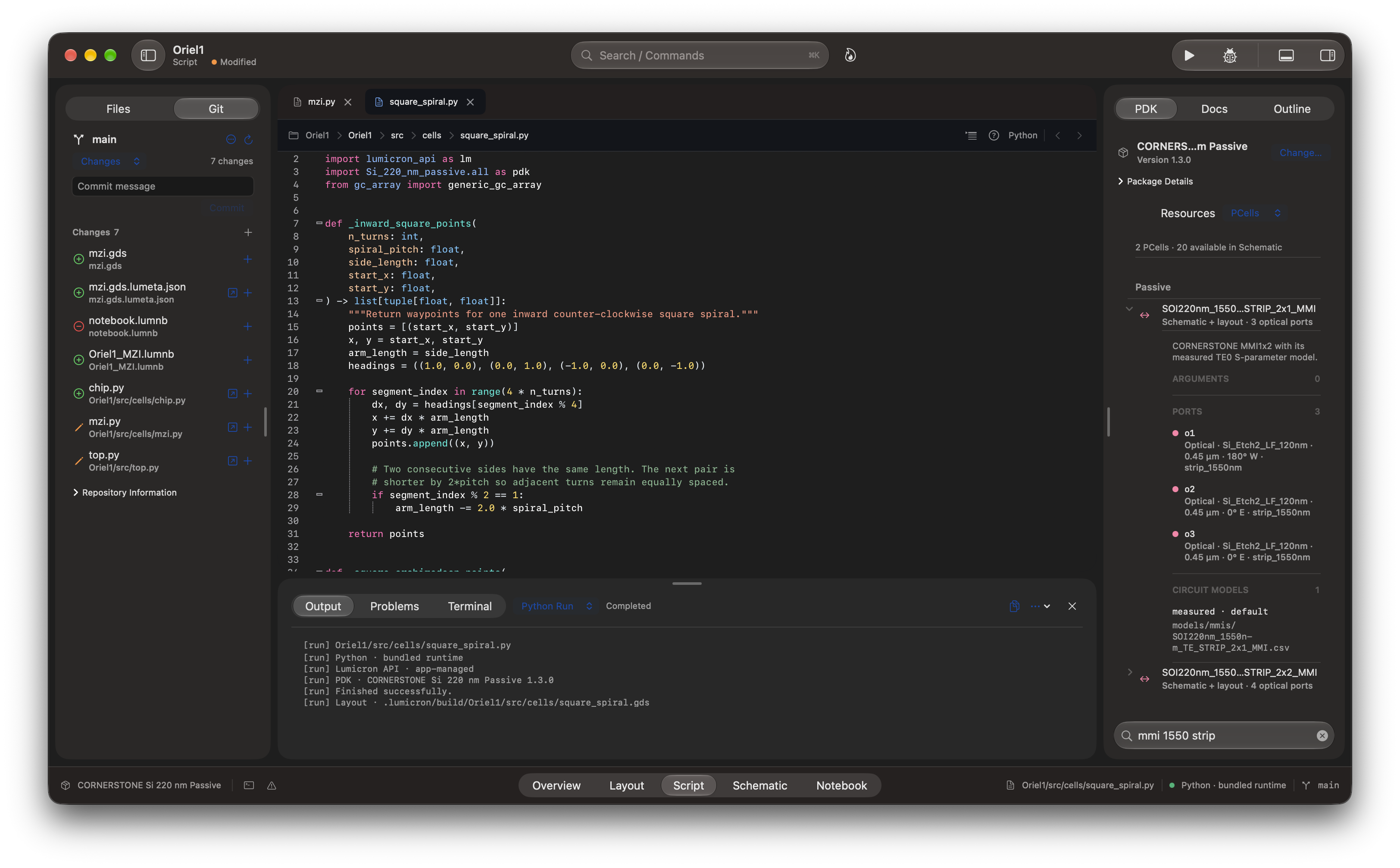
Inspect directly. Automate in Python. Both act on the same PDK-aware project.

Lumicron graphical layout workspace
Direct interaction
Same project
Lumicron Python source workspace
Readable Python

Phoebe

Project-aware intelligence,
inside Lumicron.

Fully functional offline. Connect online to a commercial AI provider of your choice when you want frontier capabilities.

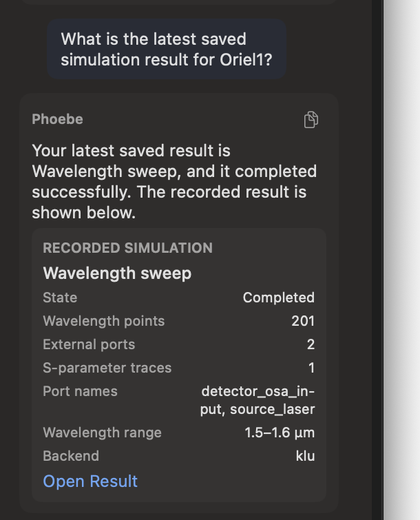
Phoebe can inspect the current project’s source, PDK, layout, schematic, and saved results through the access you grant. Here, it answers from Oriel1’s recorded simulation.

Oriel1 projectFull Oriel1 project overview with the Phoebe panel and saved simulation result visible
Magnified product detailPhoebe · Saved result
Phoebe answers the Oriel1 question with a completed wavelength sweep and 201 recorded wavelength points
Oriel1 stays in view while Phoebe identifies the latest saved wavelength sweep and its recorded result.

Take the layout
to the lab.

Design on Mac. At the probe station, use the iPad companion to navigate a chip, locate devices, and record supported measurements in layout context.

Download on the App Store

What will you design next?

Tell us about your PIC workflow.

Talk to the Lumicron team